


Cleanroom News, Cleanrooms
Apple’s A12 Bionic Chip Races Out of the Cleanroom!

Mar
What do we talk about when we talk about Apple? Perhaps it is no longer surprising that the devices and consumables that most readily spring to mind when we hear of the 11th most profitable company in the world (behind a spill of oil producers, Warren Buffet’s Berkshire Hathaway, and the perennial love-to-hate behemoth, Walmart) are not the ones that built the empire.(1) They are no longer personal computers like the Macintosh that wowed a generation of proud geeks with their then revolutionary graphical user interface (GUI), integrated screen, and built-in mouse. Nor yet are they the descendants spawned from that initial product. When we talk about Apple today, the item that springs most readily to mind today is one that no longer sits on our desk but which we now carry in our pocket, or the waistband of our Lululemons: the cellphone.
Yes, that erstwhile communications device of the rebels and present-day must-have status symbol is everywhere but, given the seeming ubiquity of the device, it may come as a surprise that Apple was not the first player in the mobile communications market. That particular award goes to Motorola when, in 1973, Martin Cooper – a researcher and executive with the company – placed the world’s first cellphone call to Joel Engel of Bell Labs. The call was made on an early prototype of the DynaTAC 800x, a consumer device that launched in 1983 while Apple’s focus was all about the ‘Lisa,’ a $9,995 box which successfully brought the concept of the GUI to personal computing. And the DynaTAC was – by modern day standards – a monster. About the size of ‘a foot long sub from Subway,’ the phone retailed for around $4000 and had a battery life of just 30 minutes.(2) In those days, it paid to talk fast.
So how have we gone from a ‘mobile’ phone the size of a standard hoagie roll to one with the dimensions of a generous crouton?
And why are folks from CNet to FastCompany so excited that Apple’s ‘best new product’ is neither a computer nor a phone? In short: what is the big deal about Apple’s tiny new innovation?
Chips. In and of themselves they may not have the ‘X-factor’ – the slickness, the gloss and glamor – we associate with mobile technology but they are what makes it perform.
Think of them as the workhorses of the product, powering it through the countless operations it executes every day. And the biggest thing about these chips is actually how small they are. Readers versed in medieval studies will remember the conundrum – a metaphysical question that is perhaps the best-known example of a reducio ad absurdum – about the number of angels that could dance on the head of a pin. Well, in some ways contemplating the development of new microprocessor chip sets is a bit like that. The processors that drive computing devices perform using transistors – components that allow chips to store and manipulate binary data. The key to a transistor’s speed and efficacy is its size: the smaller they are, the faster they can change values. So in order to understand the huge significance of the tiny transistor, let’s look at some statistics…
We’re going to be talking about how the transistors on Apple’s new A12 Bionic chip are just 7 nanometers in length but what is a nanometer?
Let’s work backwards: a centimeter is 1/100th of a meter; a millimeter is 1/1000th of a meter; a micrometer – also known as a micron – is 1/1,000,000 of a meter; and finally a nanometer is 1/1,000,000,000 of a meter. In other words, each measurement is 1000 times smaller than the one preceding it. As an example, imagine the cross section of a human hair. That’s what 75 microns look like – pretty slender but still positively gigantic in comparison with the 7 nanometer transistor. In fact, as Stephen Shankland writes in an article published by Cnet, a human hair is ‘still thick enough to fit about 10,000 of an A12’s components across its width.’(3) Still need a visual? Head over to the graphical representation in our Learning Center.
But why is getting to grips with the relative sizes of microns and nanometers so important? Well, in terms of semiconductor manufacturing, the distinction between the two scales of measurement is arguably what built the industry. In 1971, the first significant milestone was reached in the development of the 10-micron process. From there, it took 18 years to break the nanometer threshold, with the 800nm process attained by 1989. By the early years of this century, the process had reached 130nm (2001), dipping into double digits (90nm) by 2004. And finally 2018 saw the semiconductor device fabrication processes attain single digits with the launch of the 7nm process.
All of which is to say that, although it’s been many years in the making, semi-conductor technology has come a long way since the 1970 Intel 4004, the first 4-bit chip developed with an eye to the Asian market. The 30 years between 1970 and the turn of the century represent what’s come to be affectionately termed the ‘golden age’ of semiconductor chip development according to Mark Bohr who headed up Intel’s process architecture and integration. According to an interview published in The Register, Bohr recalls the halcyon days when changes in materials were rare and advances in transistor density and power were made simply through scaling.(4) But of course that model can only be pursued so far and, as Bohr recounts, ‘Traditional scaling ran out of steam […] We just plain ran out of atoms.’(5) And the reason for this dilemma is the incredible thinness of the deposit. With traditional metal-oxide gates, a 1.2 nanometer deposit is just 6 – yes, that’s six – atoms thick. And when you’re measuring the size of an object by counting its atoms, it’s safe to say both that it is incredibly small and, assuming no dancing angels, you could fit many, many of its kind onto the head of a pin.
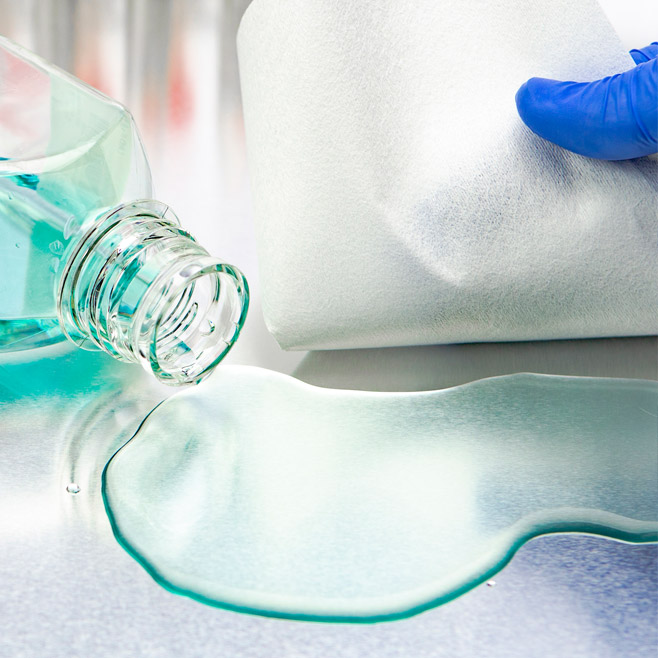
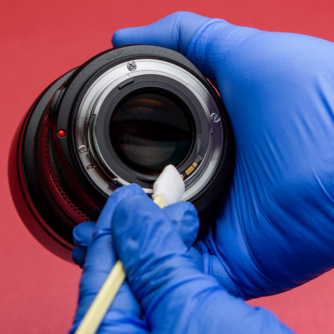
Which is big news for Apple’s new chip as the A12 packs in 6.9 billion transistors of 7 nanometers in size. Yes, you did read that correctly – six point nine billion. Running a six core central processing unit (CPU), the A12 which debuted in iPhones in September 2018 offers Vortex, a pairing of 2 high performance cores running at 2.49 GHz, and Tempest, an array of 4 energy-efficient cores that allow for extended battery life. A performance controller shares the workload across all six of the cores dynamically, utilizing the full complement when extra power is needed. The 64-bit, ARM-based system on a chip (SoC) found its way into the iPhone XS, XS Max, and XR, allowing the devices to run 15% faster and up to 40% more efficiently than preceding models.(6) Which is great for Apple and also for Taiwan Semiconductor Manufacturing Company, Limited (TSMC) which manufactures the chip. Basing its operations in Hsinchu, Northern Taiwan, TSMC was founded in 1987 and has become the world’s leading semiconductor foundry with fabrication plants around the country and offices in Asia, Europe, India, and North America.(7) The fabrication plants – also known as ‘fabs’ – serve an alphabet soup of tech customers from Apple to Xilinx and TSMC invested around $9.3 billion in the construction of the gigafab in Central Taiwan. And, of special significance to us, is the proportion of the budget devoted to cleanroom facilities. It goes almost without saying that a contamination-controlled environment is essential for a manufacturing process wherein even the most minute speck of dust or particulate matter can ruin a product. So HEPA filtration is one of the most critical components of maintaining a clean environment. Wafer fabs typically use a sub-Class 1 to Class 10 cleanroom where particles of the 0.1 micron to 0.5 micron are permissible in very small numbers. The assembly process preceding die encapsulation requires a Class 10 facility but the post-encapsulation and testing processes demand the less stringent regulations of the Class 100 filtration capacity.(8)
And then there are further considerations such as vibration control to ensure that the nanometer-scale alignment of machines remains correct, and measures to prescribe exact temperature and humidity levels – variables that are essential to minimizing the destructive effects of static electricity build-up or discharge. Moreover, once infrastructure concerns are addressed, there’s also the equipment. In cleanrooms for semiconductor development we’d expect to see, for instance, step-and-repeat cameras – ‘steppers’ – for use in photolithography. Photo- or optical lithography is the process whereby light transfers a geometric pattern onto a substrate using a photoresist. Subsequent chemical treatments either engrave the pattern into the material or allow a new layer of material to be deposited upon it and the process can be calibrated to nanometer accuracy. In addition, cleanrooms such as those owned by TSMC will likely also contain doping machines which intentionally introduce ‘impurities’ with the aim of regulating structural, optical, or electrical properties. Additionally, in terms of integrated circuits, there will also be wafer dicing machines which cut individual die from the processed wafer before being placed into chip carriers for subsequent use. And these machines do not come cheap. The typical cost for the most common pieces of equipment for semiconductor cleanrooms starts at around the $700,000 mark and climbs from there. A stepper, for example, can reach as much as $130 million – and manufacturers like TSMC will generally require several in each fab.
So with this kind of cost in mind, how are the new A12 Bionic chips actually benefitting from their time in these state-of-the-art, phenomenally expensive cleanroom facilities? We’re glad you asked because we’re about to get geeky again.
The A12 Bionic leverages a new design with a double-gate structure incorporating the fin-shaped components. Using a FinFET process, the field-effect transistor builds upon the concept of the metal-oxide-semiconductor field-effect transistor (MOSFET) but adds the all-important double-gate to achieve faster switching times. Moreover, the process still allows a reduction of gate width to just 50 nanometers and gate thickness to a supremely slender 5 nanometers. The faster switching time gives a significant boost to the degree of raw processing power of the A12, enabling the creation of a neural engine that actually facilitates machine learning. Phil Schiller, marketing chief at Apple, noted that the use of artificial intelligence at the device level is based squarely upon the chip which enables the smart compute system to ‘analyze the neural network data and figure out on the fly whether to run it on the CPU, the GPU or the neural engine.’(9)
And in Apple’s terms, ‘on the fly’ is incredibly fast. Up to 5 trillion operations per second fast. Which is what allows a device – in this case the latest generation of iPhones – to function in an eerily human way, not just taking better ‘selfies’ but also recognizing patterns, making predictions, and even learning from its experiences. The much-touted ability of Apple phones and wearables to recognize and alert to irregular or potentially dangerous heartbeat patterns, for instance, relies upon this level of processing capacity.
Does all of this sound like sci-fi? Perhaps, but it is real world science and we are not the first to notice the degree to which technology is bringing the future into the present. As Ben Bajarin, analyst for consumer technology products at Creative Strategies, noted: ‘“Apple is getting dangerously close to bringing a great deal of science fiction into reality and the efforts they are doing with machine learning is at the center.”’(10) And for our purposes, it is worth noting that at the center of Apple’s machine learning capacity is a chip that was born of our industry, of a state-of-the-art cleanroom equipped with mind-blowing technology and superlative consumable products. And, in all of the celebrations around Apple’s latest innovation, we think that key point – the role of the cleanroom – is worth its very own moment in the spotlight.
What do you think? Are you as excited by this semiconductor innovation as we are? Or are you resisting the siren call of the newest shiny Apple bauble? We’d love to hear from you – so let us know your thoughts in the comments!
References:
- https://fxssi.com/top-10-profitable-companies-world
- https://bebusinessed.com/history/history-cell-phones/
- https://www.cnet.com/news/iphone-xs-industry-first-a12-chip-gives-apple-big-advantage-over-rivals/
- https://www.theregister.co.uk/Print/2011/11/15/the_first_forty_years_of_intel_microprocessors/
- ibid
- https://www.apple.com/iphone-xs/a12-bionic/
- Interestingly TSMC also manufactures a FinFET chip for an Apple competitor, Chinese company Huawei, which unveiled its own 7-nanometer chip, the Kirin 980, just days before Apple shipped the A12-enabled iPhones.
- http://eesemi.com/cleanrooms.htm
- https://www.cnet.com/news/iphone-xs-industry-first-a12-chip-gives-apple-big-advantage-over-rivals/
- ibid

HAVE AN IDEA FOR CONTENT?
We are always looking for ideas and topics to write about.
Contact Us